


Table of Contents
The p-type silicon wafer is a fundamental material in the semiconductor and photovoltaic industries, forming the backbone of many modern technologies. It is widely used in solar cells, integrated circuits, and power electronic devices due to its stable electrical behavior and cost-effective manufacturing process. By introducing boron as a dopant, the p-type silicon wafer creates positive charge carriers (holes), which play a key role in controlling current flow. Its balance of performance, scalability, and reliability makes it one of the most important substrates in both renewable energy systems and electronic applications.
1. How a p-type silicon wafer improves solar cell performance
In solar energy systems, the p-type silicon wafer serves as the base layer for most conventional photovoltaic cells, directly affecting conversion efficiency and long-term stability.
- Formation of efficient p-n junctions:
The wafer works as the base region where an n-type layer is added on top, creating a p-n junction. This structure allows sunlight-generated electrons and holes to separate efficiently, reducing recombination losses and improving energy output. - Enhanced light absorption capability:
The crystalline structure of the p-type silicon wafers supports strong photon absorption. This ensures that more sunlight is converted into usable electrical energy rather than being wasted as heat. - Cost-effective solar production:
Compared to alternative semiconductor materials, p-type substrates are easier to manufacture at scale. This reduces overall solar panel production costs, making renewable energy more accessible. - Stable long-term outdoor performance:
Solar modules using this wafer type demonstrate strong resistance to environmental stress, including UV exposure, humidity, and temperature fluctuations, ensuring consistent output over decades.
2. Electrical advantages in semiconductor devices
In electronics manufacturing, the p-type silicon wafer is widely used because of its predictable electrical characteristics and compatibility with various device structures.
- Controlled hole concentration for circuit design:
The boron doping process allows precise adjustment of carrier density. This makes it easier to design transistors and integrated circuits with stable switching behavior. - Reliable integration with n-type regions:
Most semiconductor devices depend on p-n junctions. The p-type silicon wafer integrates seamlessly with n-doped silicon, enabling diodes, MOSFETs, and logic circuits to function efficiently. - High production yield in fabs:
Manufacturing processes using p-type substrates tend to produce fewer defects, increasing chip yield and reducing production waste. - Balanced electrical performance:
It offers a practical combination of conductivity, resistance control, and thermal behavior, making it suitable for both analog and digital electronic systems.
3. Material characteristics that make a p-type silicon wafer reliable
The performance of the p-type silicon wafer is strongly linked to its physical and chemical properties, which ensure durability and consistency across applications.
- Uniform crystal structure:
The wafer is produced from high-purity silicon ingots, ensuring minimal defects and consistent atomic alignment, which improves device reliability. - Adjustable resistivity range:
Manufacturers can fine-tune resistivity levels depending on application needs, from low-power sensors to high-power photovoltaic modules. - Thermal endurance under harsh conditions:
It maintains electrical stability even at elevated temperatures, making it suitable for industrial and automotive environments. - Mechanical strength during processing:
The wafer can withstand cutting, polishing, and etching processes without significant damage, supporting high-volume semiconductor fabrication.
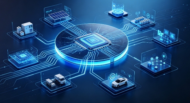
4. Industrial applications across multiple sectors
The p-type silicon wafer is not limited to solar and consumer electronics; it plays a major role in several high-tech industries.
- In renewable energy systems, it is the dominant material used in large-scale solar farms and residential photovoltaic panels, supporting global clean energy transition efforts.
- In consumer electronics, it is used in smartphones, computers, and wearable devices, forming the basis of integrated circuits and memory components.
- In automotive electronics, it supports sensors, engine control units, and power management systems in electric and hybrid vehicles, where reliability is critical.
- In industrial automation, it is applied in power converters, motor controllers, and smart manufacturing systems that require stable and efficient electronic control.
Each of these applications benefits from the wafer’s stability, scalability, and compatibility with existing semiconductor manufacturing technologies.
Conclusion
The p-type silicon wafer remains a cornerstone material in both the solar energy and semiconductor industries due to its excellent balance of cost, performance, and reliability. It enables efficient solar energy conversion, supports advanced electronic device fabrication, and meets the demands of multiple high-tech sectors. As global industries continue to move toward renewable energy and smarter electronics, the importance of the p-type silicon wafer will continue to grow, making it a key driver of future technological innovation.
0